Full Adder Circuit Diagram Ppt
Adder circuit half carry bit ripple schematic diagram logic gate truth table perform digital delay without xor doubt computer input Adder carry circuit sum logic implementation output electronics simplified two outputs combinational circuits tutorial both shows below figure Adder cmos circuit diagram transistor fa 28t transistors implementation edacafe using transmission gate power fig phdthesis www10 book
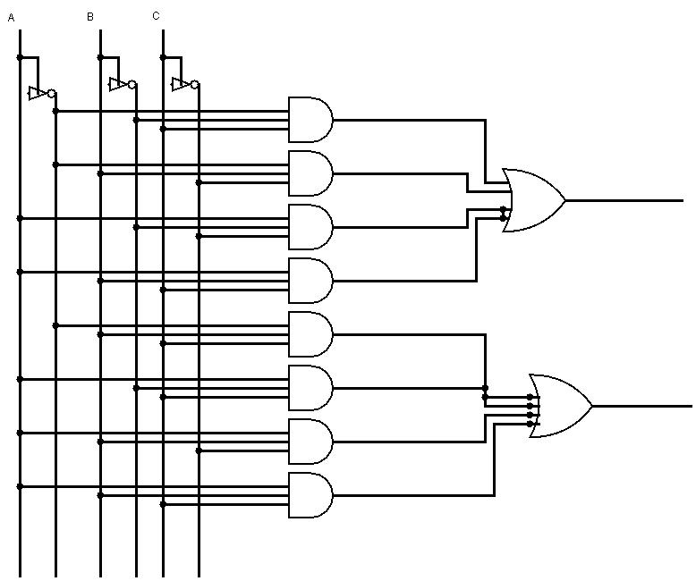
New Full adder circuit | Download Scientific Diagram
Adder circuit What is adder? Adder half implement inputs
New full adder circuit
Adder arithmetic circuits circuit andrew element diagramFull adder circuit diagram Block diagram of full-adder circuitAdder gates.
Figure 1: schemaric of a full adderSystem description of the full-adder circuit shown in fig. 1 Adder circuit2.2: proposed full adder circuit.

Adder combinational logic circuits
Adder classificationsCombinational logic circuits : definition, examples, and applications Adder figure diagramFull adder conbinational circuit ~ all computer topics.
Vhdl code and circuit diagram for full adderAdder xor rangkaian transistor ripple pengertian kombinasi Adder diagram circuitOptimized full adder circuit diagram.

Full adder circuit diagram
Circuits and arithmeticAdder in digital electronics, half adder and full adder in digital Edacafe: power, accuracy and noise aspects in cmos mixed-signalAdder circuit schematic diagram.
Full-adder circuitFull adder Adder circuit proposedAdder circuit diagram vhdl code.

Complete circuit of the full adder using the newly proposed design. the
Adder half circuit digitalAdder circuit Full-adder circuit, the schematic diagram and how it works – deeptronicFull adder circuit diagram.
Adder circuit construction binary circuits qiskit sourav guptaAdder circuit diagram simplification computer Full adder circuit: theory, truth table & constructionProposed full adder schematic diagram.

Design and implement half adder and full adder.
What is half adder .
.

Complete circuit of the full adder using the newly proposed design. The

Full Adder Circuit Diagram

EDACafe: Power, accuracy and noise aspects in CMOS mixed-signal

Full-adder circuit

Block diagram of full-adder circuit | Download Scientific Diagram

Proposed full adder schematic diagram | Download Scientific Diagram

Full Adder Circuit Diagram